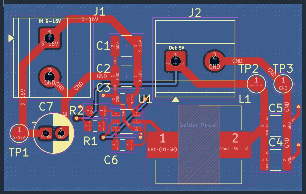
Overview
Developed a two-layer PCB for a 9–16 V input supply targeting 5 V at 1 A. The project applied buck-converter theory to schematic capture, component and footprint selection, placement, routing, and manufacturing exports.
J1 and J2 use through-hole screw terminals for supply and load wiring. Three exposed copper test pads provide VIN, VOUT, and GND access for planned bench measurements.
Component Selection
Selected the TI LMR51420XFDDCR synchronous buck regulator for its 4.5–36 V input range and 2 A output-current capability, providing operating margin around the 9–16 V, 1 A design target. Its integrated high-side and low-side MOSFETs simplify the external power stage.
Used the datasheet's 5 V application circuit as a starting point for L1, C4–C6, and the feedback divider. The final schematic combines local input bypassing, bulk input storage, and parallel output capacitors.
| Component | Selected value | Design role |
|---|---|---|
| L1 | 10 µH | Stores energy and smooths the current delivered from the switching stage. |
| C4, C5 | 22 µF each | Provide 44 µF nominal output capacitance. The parallel pair lowers combined ESR and supports output-voltage filtering and load transients. |
| C6 | 100 nF | Bootstrap capacitor between CB and SW that supplies the floating high-side gate driver. |
| C1, C2 | 4.7 µF each | Parallel ceramic input bypassing provides local charge for switching-current pulses. |
| C3 | 100 nF | Local high-frequency input bypassing, placed near the regulator. |
| C7 | 22 µF | Polarized bulk input capacitor adds energy storage for input-current transients. |
Output Voltage Setting
R1 connects VOUT to the FB node, and R2 connects FB to ground. The regulator controls the switching stage to hold FB near its nominal 0.600 V reference. With R1 = 100 kΩ and R2 = 13.7 kΩ:
VOUT = VREF × (1 + R1 / R2)VOUT = 0.600 × (1 + 100 / 13.7) ≈ 4.98 V
This is the calculated nominal setpoint; actual output regulation remains a planned bench measurement.
Regulator specifications and nominal reference: TI LMR51420 datasheet, sections 7.5 and 9.2 .
PCB Layout
Used wider traces for power connections to reduce resistance and voltage drop, with narrower routing for feedback and enable signals. Placement and routing prioritized two connections:
- Input bypass return: Kept C3 pad 2 close to U1 pad 1 (GND) to minimize inductance in the local switching-current return.
- Switch node: Kept U1 pad 2 (SW) to L1 pad 1 short to limit connection inductance and switching-node copper area.
To preserve these paths, routed the output-sense connection from R1 pad 1 to J2 pad 1 and the enable connection from U1 pad 5 to VIN at pad 3 on the bottom copper layer.
Layout checks: Zero DRC violations, unconnected items, or schematic mismatches were reported for the enabled checks. Gerber and drill exports were reviewed.
Planned Verification
Bench verification is planned across input-voltage and load conditions.
| Check | Planned Measurement |
|---|---|
| Output regulation | How closely VOUT holds the 5 V target as VIN and load change |
| Ripple | Output ripple using a short oscilloscope ground connection |
| Startup | Output rise, overshoot, and behavior under load |
| Efficiency | Output power divided by input power across operating points |
| Thermal behavior | Temperature rise at the regulator and inductor under sustained load |
Project Notes
The three-page document includes the schematic, footprints, routing decisions, and design-check results.