Overview
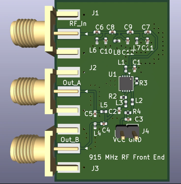
Designed a 902–928 MHz receiver front end with band-pass filtering, low-noise amplification, and complementary outputs for a differential input.
Scope includes circuit simulation, impedance matching, vendor-model evaluation, schematic capture, footprint selection, and four-layer PCB layout. The ADC and downconversion stage are external.
RF Circuit Design
LC Balun
Compared ideal and vendor LC balun models against a target of less than 0.5 dB amplitude imbalance. Adjusting the capacitors from 2.5 pF to 2.4 pF improved the modeled output balance.
LNA Stability & Matching
The initial amplifier model was conditionally stable. Added damping improved simulated stability at the cost of gain. S-parameter analysis determined the target source and load impedances for the matching networks.
Replaced ideal components with Coilcraft and Murata models to evaluate loss and parasitic effects.
Band-Pass Filter
Designed capacitively coupled LC resonators around 915 MHz with a 100 MHz bandwidth target. Retuned resonator capacitances after vendor models shifted the response and increased loss.
PCB Layout
Selected a four-layer, 1.6 mm construction with both inner layers assigned to ground for continuous RF return paths.
| Layer | Use |
|---|---|
| F.Cu | RF components, RF routing, and adjacent ground copper |
| In1.Cu | Main RF ground reference |
| In2.Cu | Ground reference for bottom-layer routing |
| B.Cu | DC power routing and ground copper |
Grounded coplanar waveguide geometry uses a 0.3058 mm trace width and 0.20 mm ground gap for the selected stackup. Final impedance depends on manufactured geometry.
Placed matching components near the amplifier, added ground vias at shunt components, and stitched ground along sensitive RF connections. Similar balun branch lengths limit additional phase imbalance.
Output routing: Out_A is 10.6344 mm and Out_B is 10.4597 mm in the layout, a difference of approximately 0.175 mm.
Simulation Results
Combined-circuit simulations evaluate gain, output phase and amplitude balance, and impedance matching. The simulated −3 dB bandwidth is approximately 102.5 MHz, spanning 867 to 969.5 MHz.
Planned Verification
Planned hardware checks cover input matching, frequency response, gain, output balance, and power behavior. ADC integration requires checking input frequency, drive level, common-mode voltage, and output conditioning.
Project Report
The 25-page report documents simulations, component selection, matching calculations, schematics, stackup, and PCB layout.